
Switches with Integrated Optics based interconnects are becoming essential to meet the bandwidth-density and power efficiency requirements of next gen AI infrastructure.
Copper based interconnects with reaches of 5-7m have been the dominant method of connecting compute elements within “AI factory” datacenters. Let’s examine the benefits of integrated optics and why it becomes essential as we move from link speeds of 212Gbps to 448Gbps. This blog, https://650group.com/blog/the-widening-chasm-xpu-data-hunger-outpaces-network-infrastructure/, explains the problem statement and opportunity.
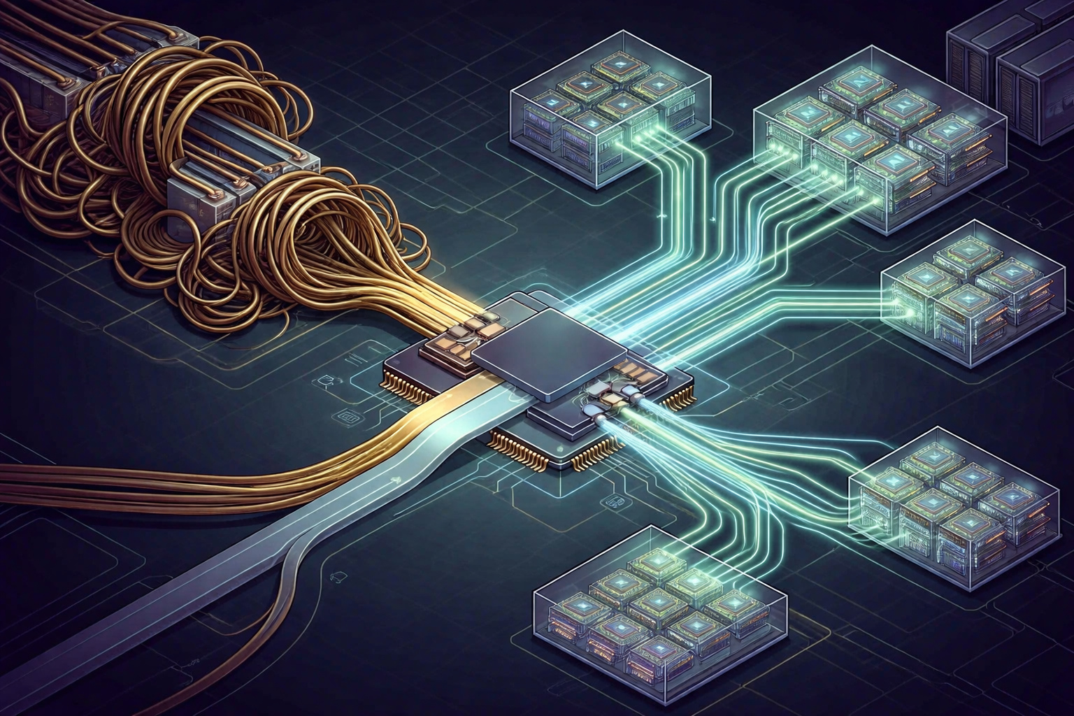
Passive copper based interconnects have provided low cost, power and latency connectivity for tightly coupled configurations of 72 to 144 compute elements within a rack. However, as AI applications scale to 1000+ compute elements, single rack configurations are giving way to multi-rack configurations. Even with the increased rack width and cooling capabilities of ORV3 racks, the sheer volume of links and the increase in link distances necessitate power hungry DSPs and retimed copper based solutions.
As an example, for 576 GPU based systems that are expected to span 4 racks, copper cabling becomes unwieldy. For reaches of 5-7m, the cable gauge and thickness required to support high data rates consumes critical chassis real estate, directly reducing clustering density.
It is expected that by 2027 interconnect distances that are well past the practical limit of copper solutions will be required. Copper solutions also constrain the bandwidth density per system: Even with the densest connectors available, the highest practical bandwidth achievable in a 1OU form factor is expected to be 102.4T with copper.
AI networks using traditional copper interconnects are hitting a bandwidth-density and reach “wall”. Systems utilizing integrated optics offer a viable path to overcoming these obstacles due to the inherent properties of optics compared to copper: Bandwidth density is increased since optical fiber density far exceeds electrical cable density, and optical technologies enable further reach at higher speed than is achievable with copper.
However, any solution that overcomes the bandwidth-density and reach limitations of copper also need to meet the cost, power and reliability that copper interconnects have provided. This blog explores how integrated optics can meet these challenges, and enable next generation AI networks.
Comparing integrated optics to pluggable optics
Traditionally, switch systems have used pluggable front-panel optical modules in form factors such as OSFP and QSFP-DD. In the latest 102.4T switch systems, the electrical interface between the switch silicon and front pluggable modules consist of high speed differential PCB traces running at 212Gbps. Switch systems are typically shipped with “empty” front panel ports, and optical transceivers are installed by the customer at the time of deployment. 800Gbps modules are shipping at volume today and 1.6Tbps modules are expected to ship in high volume starting Q2, 2027.
Pluggable modules can be replaced in the event of failure, but require power-hungry DSPs to compensate for the electrical channel losses of the PCB traces between the switch silicon and front panel. Depending on the transceiver architecture and DSP technology node used, 1.6T module power can range from 14-25W (8.75pJ/bit to 15.6pJ/bit).
In contrast, Integrated optics systems feature optics that are assembled within the switch chassis at the time of manufacture. This allows the optical engines to be placed in close physical proximity to the switch silicon, reducing electrical trace lengths and eliminating the need for high-power DSPs.
The two most common implementations of integrated optical systems are Near Packaged Optics (NPO) and Co-Packaged Optics (CPO). For both implementations the laser source can be integrated into the optical engine, or be disaggregated and front-panel pluggable, enabling replaceability in the event of a laser failure – just like the traditional modules. Fig 1 below illustrates NPO and CPO implementations.
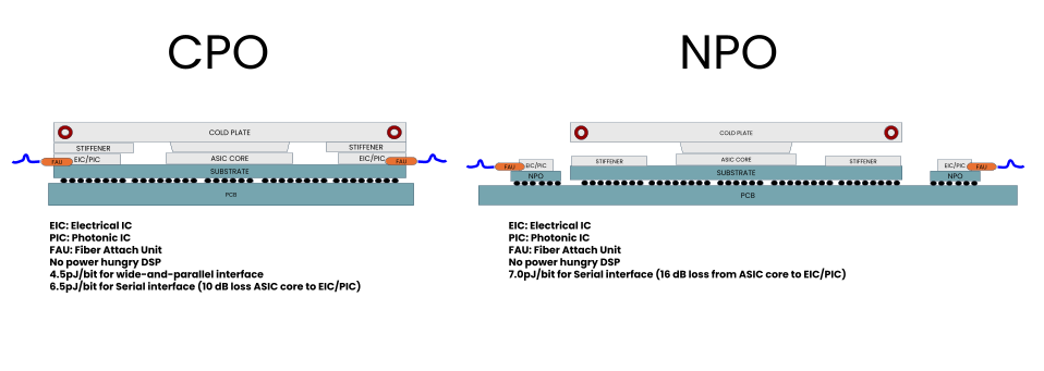
Fig 1: Co-packaged and Near Packaged Integrated Optics
Reducing power consumption with integrated optics.
In first generation CPO and NPO systems, power reduction is achieved by eliminating power intensive DSPs traditionally required for pluggable optics. Depending on the specific technologies used, optical power consumption for CPO and NPO systems can be reduced to between 7W – 11W per 1.6T (4.4pJ/bit – 6.9pJ/bit) – roughly half that of comparable pluggable optical solutions. Eliminating the DSP also eliminates any additional latency, since what remains is a fully linear path from the switch silicon to optical output.
In current CPO and NPO implementations, the optical engines connect to the switch silicon using short electrical channels running at 212Gbps PAM4. In order to support electrical I/O at 212 Gbps, switch ASICs include 212G PAM4 SerDes (Serializer / Deserializer) macros. The high-speed SerDes macros convert the ASIC’s internal wide & parallel interface into high-speed serial I/O running at 212 Gbps. While these SerDes blocks are versatile – supporting everything from passive copper to retimed optics – they carry a power footprint of ~5W to 8W per 1.6T (~3 to 5 pJ/bit), depending on implementation and vendor.
Next generation CPO designs can eliminate the SerDes layer entirely, allowing the ASIC’s internal wide-and-parallel interfaces to drive optical engines directly. Replacing the switch SerDes with a wide-and-parallel interface reduces the electrical I/O power to ~800mW per 1.6T(< 1 pJ/bit). Optical engines driven by these wide-and-parallel interfaces are expected to consume only ~4W – 6W per 1.6T (~ 3-4 pJ/bit). Adding the switch electrical IO power and the optics power results in an astonishing total power consumption of only 4.8W – 6.8W per 1.6T. For the first time, optical interconnects are now poised to achieve power-parity with passive copper interconnects, eliminating a key barrier to adoption of optics for scale-up applications.
With the power barrier removed, let’s now explore cost efficiencies unlocked by integrated optical solutions.
Reducing Cost with Integrated Optics
In CPO systems, optical engines are integrated onto the same substrate as the switch silicon. The “siliconizing” of optics leverages a rapidly maturing semiconductor ecosystem, driving interconnect costs down towards a target of ~ 10c per Gbps. For example TSMC’s COUPE (Compact Universal Photonic Engine) technology is being used in many leading co-packaged systems. Furthermore, because the silicon substrate internalizes all high-speed signal routing, the CPO package can be mounted on simpler PCBs. This can lower PCB costs by 50% to 60% when compared to traditional architectures that require expensive, high-layer-count boards to maintain signal integrity over long electrical traces.
With NPO, costs are reduced through the elimination of DSPs, simple assembly procedures, efficient PCB panelization due to integration, and the consolidation of mechanical & thermal components.
In both approaches, the system is fully stress-tested, with optics, at the time of manufacture. This allows customers to deploy systems rapidly, completely eliminating costly optics qualification cycles, and the time taken to physically handle and install many thousands of optical modules by hand. The reduction in deployment time lowers the total cost of ownership, and reduces the time-to-revenue of multi-billion dollar AI infrastructure builds.
Integrated optics & reliability
A common industry concern regarding CPO and NPO systems centers on serviceability and Mean Time to Repair (MTTR), as these systems lack the piece-wise replaceability of traditional front-panel pluggable systems. However, this perspective often conflates replaceability with reliability. Integrated architectures offer several structural advantages that can improve reliability and overall cluster uptime.
First, the end-to-end link performance of CPO & NPO systems can be comprehensively tested over process and temperature corners by the system vendor at the time of assembly. This creates a traceable record of “time zero” performance, and ensures that each optical link of the system is 100% tested and validated before the switch ever reaches the data center. This stands in contrast to systems that use pluggable optics, where systems ship without the optics installed, and where the performance of any individual system + optics can only be verified at the time of deployment.
Second, system architectures that incorporate redundant or disaggregated (replaceable) laser sources can further improve the overall system MTTR.
Third, leading hyperscalers have already started validating the reliability of integrated optical systems. For example, recent tests results from Meta have validated over one million flap-free CPO port hours, demonstrating the stability of CPO systems in a production environment. We expect that by the end of 2026, the industry should have sufficient data to statistically support the thesis of the higher reliability of integrated optics due to the reduction in failure points of pluggable optics.
These trials should help dispel concerns and overcome the assumption that replaceability of pluggable optics is the same as reliability. It is incumbent upon systems vendors to prove the reliability of these integrated optics based switches by working with the hyperscalers and customers who benefit the most. The future of scalable AI factories will hinge on this advancement.
Conclusion
At Nexthop AI we believe that integrated optics is a viable and manufacturable solution to meet next generation connectivity needs at scale. We are exploring a range of solutions, including novel architectures that enable mixing and matching of optical interface media-types, such as DR and FR optics. In 2027, the power per link is expected to be ~7W per 1.6T and, as volumes ramp, costs are expected to be driven down to less than 10c / Gbps. These are exciting times – Stay tuned !